Chip Packaging
Contents
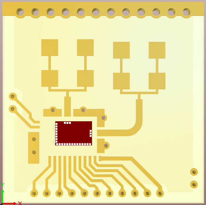
1 Bare Die Bonded to PCB
It is the simplest method to evaluate the MMICs as well as sample productions for small quantities. Chip is glued directly on the printed circuit board (PCB) with or without using a cavity. Then, gold or aluminum wire bonds are used to make the electrical connections from the pads of the chip to the lines on the PCB. Optionally, a glop-top procedure can be applied to protect the chip and the wire bonds from damage.
Advantages:
- Can be custom to each MMIC allowing very short bond wires for RF pads
- Wafer probe testing of MMIC is possible
Disadvantages:
- Full chip functionality cannot be tested, since the MMIC is not in a package that is suitable for an industrial socket
- MMIC is not replaceable on the PCB
- Not suitable for series production
2 Flip Chip
Flip chip is another method to evaluate the MMICs, as well as sample productions for small quantities. Solder bumps or stud bumps are placed on the pads of the MMIC. Then, MMIC is directly placed on the printed circuit boards (PCB), and soldered. This allows very short connection from pads of the chip to PCB; however pitch between pads must be kept 300-400um wide to fit the standard PCB technology requirements. This makes the MMIC bigger for complex designs.
Advantages:
- Low cost
- No requirement for bond wires
- Good RF performance
- Suitable for series production and series testing
Disadvantages:
- Requirement for high pitch between pads making the MMIC bigger
- Not suitable for standard footprints such as QFN
- Harder to make series tests
- More expensive than a standard QFN
3 (FAM) QFN
3.1 Quad-flat no-lead (QFN)
Quad-flat no-lead (QFN) is one of the standard packaging technologies used in electronics. MMIC is wire bonded to a pre-produced lead frame. Then, whole package is molded on top with plastic. Having 0.4mm to 0.6mm pitch, it is easy to handle for surface mount technologies (SMT) for assembly printed circuit boards (PCB). For more detailed information: Wikipedia - QFN
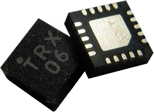
Advantages:
- Cheap and Reliable
- Suitable for series production and series testing
Disadvantages:
- Short RF bond wires are not possible
- RF signal loss due to long bond wires for RF pads
- RF signal loss over the molding material for on chip antenna versions
Since this technology is very well known and widely used around the globe, Silicon Radar is trying to keep its standard layouts even for other packaging technologies.
3.2 Film Assisted Molded (FAM) QFN
Film Assisted Molded QFN is one the series production technologies that; Silicon Radar has been using for antennas in package solutions. Antennas are manufactured on an RF material and placed next to the MMIC in the lead frame. Then RF pads are directly wire bonded to the antennas. To overcome the RF losses in the molding material as in a standard QFN package, RF wire bonds are kept short and a window is opened over the antennas using a film assisted molding technology.
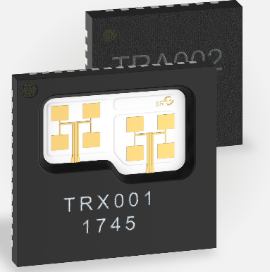
Advantages:
- Reliable
- Short RF bond wires possible
- Suitable for QFN footprint
- Suitable for series production and series testing
Disadvantages:
- Requirement for fine antenna and MMIC placement
- Requirement for careful wire bonding
- Slower in series production making it more expensive in very high quantities
- More expensive than a standard QFN
4 (FAM) LGA
4.1 Land Grid Array (LGA)
Land Grid Array (LGA) is another standard technology for packaging MMICs. Instead of using a lead-frame as used in a QFN, a printed circuit board (PCB) is used as a base for the package. Chip is placed and wire bonded on the PCB base and molded on the top. Compared to QFN, LGA allows shorter bond wires and custom antenna designs on the package, because the base PCB can be designed accordingly.
Advantages:
- Reliable, low cost and fast processing
- Short RF bond wires possible
- Suitable for QFN footprint
Disadvantages:
- Not the best RF performance
- Harder to solder on a PCB compared to lead-frame based packages
4.2 Film Assisted Molded (FAM) LGA
LGA is almost in the same method as Quad-flat no-lead (QFN) by only replacing the lead frame with a custom designed printed circuit board (PCB). Therefore, Film Assisted Molding (FAM) technology can also be used. This allows opening a window on top of the antennas to reduce the RF losses.
Advantages:
- Reliable and Low cost
- No need for fine placement of the antennas next to MMIC as in FAM QFN
- Short RF bond wires possible
- Suitable for QFN footprint
Disadvantages:
- Requirement for careful wire bonding
- Not the best RF performance
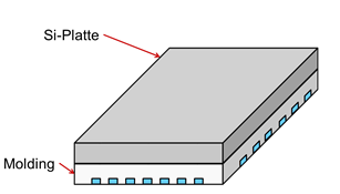
5 Silicon Package
Silicon Package is one the technologies that; Silicon Radar has been working on for antennas in package solutions. Antennas are manufactured on the RF MMIC. Therefore, there is no requirement for wire bonding of the antennas. To get the maximum signal out of the Silicon chip and antennas a silicon / high permittivity plastic lenses are designed to be placed on top of the package. To overcome the RF losses in the molding material as in a standard QFN package, a lead frame is manufactured using a silicon plate. MMIC and its antenna are directly placed on the silicon plate in the package.
Advantages:
- Reliable
- Under development to be suitable for series production and series testing (Suitable for QFN footprint)
- No need for bond wires or Film Assisted Molding (FAM)
Disadvantages:
- The layout of the first samples (5x5 Si-Package) is not compatible with standard QFN. Therefore not suitable for series testing
- Not very advantages for lower RF frequencies
6 Chip Embedding
Chip embedding with µ² technique is an advanced PCB-based technology. Rather than a standard printed circuit boards (PCB) technology with 50-100 um line and space, this technology allows down to 20 um line and space with very good tolerance. Accordingly, fine-tuned antenna structures can be designed. In addition to that, MMIC is buried into the PCB. Pads are connected to lines using copper pillars or gold stud bumps.
Advantages:
- Good RF performance
- No need for bond wires or Film Assisted Molding (FAM)
- Low cost and fast processing if the series production is started
- Suitable for multi-chip modules with high-accuracy antennas on board
- Suitable for QFN footprint
Disadvantages:
- Very expensive and long lead times for prototyping
- Harder to solder on a PCB compared to lead-frame based packages